The principle of the MC1496 analog multiplier refers to a dependent nonlinear device that multiplies two analog signals (voltage or current). It actually means that two signals that have nothing to do with each other are multiplied by an analog multiplier, that is, the output signal is proportional to the product of the input signal. The analog multiplier has two input ports, namely the X input port and the Y input port. The polarities of the two unique input signals of the analog multiplier are different. The coordinate plane of the analog multiplier uses the X-axis and the Y-axis to divide the plane rectangular coordinate system into four quadrants. When the signal depends only on a certain When only one polarity voltage can operate, the analog multiplier becomes a single-quadrant multiplier; if one of the signals can use two voltages, the two voltages are positive voltage and negative voltage, and the other of the signals only If it can work at one voltage, then the analog multiplier is called a two-quadrant multiplier; when both signals can adapt to four polarity combinations, the analog multiplier becomes a four-quadrant multiplier. A series of tests were conducted on the simulated multiplier through circuit principle expressions.
Master the working principle of amplitude modulation
Master the method of using MCl496 integrated analog multiplier to realize AM and DSB modulation and study the relationship between modulated wave, modulated signal, and carrier wave
Master the method of measuring the amplitude modulation coefficient on an oscilloscope
Learn to analyze experimental phenomena through the transformation of waveforms in experiments
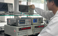
The integrated multiplier amplitude modulation circuit module is mainly composed of MC1496, and its circuit schematic is shown in the figure.
In the figure, 1W02 is used to adjust the balance between terminals (1) and (4), and 1W03 is used to adjust the balance between terminals (8) and (10). 1K01 switch controls whether terminal (1) is connected to DC voltage. When 1K01 is set to "left", terminal (1) of 1496 is connected to DC voltage, and its output is ordinary amplitude modulation wave AM. Adjusting 1W01 can change the modulation of the amplitude modulation wave. system.
When 1K01 is set to "right", its output is the suppressed carrier double sideband amplitude modulation wave DSB. Transistor 1Q01 is an emitter follower to improve the load capacity of the modulator.

AM experimental circuit composed of MC1496
The unit number of the integrated multiplicative amplitude modulation circuit in the module is 7. It is located on the left side of the sub-board, as shown in Figure 4-2.

Figure 4-2 Integrated multiplier amplitude modulation circuit sub-board (left)
Use an oscilloscope to observe the normal AM waveform and then measure its amplitude modulation coefficient;
Use an oscilloscope to observe the input offset voltage adjustment and DC modulation characteristic measurement of the integrated analog multiplier amplitude modulation circuit;
Use an oscilloscope to observe the waveform of the balanced amplitude modulation wave (double sideband DSB that suppresses the carrier)
Use an oscilloscope to observe the amplitude modulation waveforms when the modulation signal is a square wave and a triangle wave.
(1) Power on the module
Connect the integrated multiplier amplitude modulation and demodulation sub-board to power.
(2) Adjustment of input offset voltage (adjustment of AC feedthrough voltage)
1. Modulation signal source: low-frequency signal source (1KHz, 500mV, sine wave);
2. Carrier source: DDS signal source (2MHz, 500mV);
3. Input offset zero adjustment to adjust the multiplier to a balanced state. Set 1K01 to the double sideband side, add the modulation signal to 1P02. Without the carrier signal, adjust 1W03. Monitor the minimum output waveform amplitude of 1TP03; then, add the signal output from the carrier source to 1P01. Without adding the audio signal, adjust 1W02. Monitor the output waveform amplitude of 1TP03 with the smallest amplitude.
(3) Observe the DSB signal waveform
Connect the carrier output from the DDS signal source to 1P01. Connect the audio modulation signal to 1P02. Connect the oscilloscope CH1 to the amplitude modulation output terminal 1TP03. You can observe the modulation signal and its corresponding DSB signal waveform. The waveform is shown in Figure 4-3. If the observed DSB waveform is asymmetrical, the 1W02 potentiometer should be fine-tuned.

Figure 4-3 DSB signal output waveform Figure 4-4 DSB signal output waveform with lower carrier frequency
2. Observation of DSB signal inversion point
In order to clearly observe the inversion of the zero-crossing point of the double-sideband signal, the frequency of the carrier must be reduced. Set the carrier to 100KHz, 500mV. The modulation signal is still 1KHz with an amplitude of 500mV. Increase the X-axis scan rate of the oscilloscope and carefully observe the DSB signal corresponding to the zero-crossing moment of the modulation signal. The waveform at the zero-crossing moment should be inverted, as shown in Figure 4-4.
3. Phase comparison between DSB signal waveform and carrier waveform
Connect CH1 of the oscilloscope to point 1TP01, and connect CH2 to 1TP03. Compare the phases of the input carrier waveform and the output DSB waveform. It is found that they are in phase during the positive half-cycle of the modulation signal and in phase during the negative half-cycle of the modulation signal.
(4) Measuring AM (ordinary amplitude modulation) waveform
1. AM waveform observation
On the basis of maintaining the input offset voltage adjustment, set 1K01 to the "normal amplitude modulation" side. Carrier wave (2MHz, 500mV), modulation signal (1KHz, 500mV). Connect CH1 to 1TP02 and CH2 to 1TP03 on the oscilloscope. You can observe the normal AM waveform, as shown in Figure 7-5. The frequency and amplitude of the modulation signal and the carrier signal need to be adjusted at the same time. When the frequency of the carrier signal is adjusted to 10KHz, the waveform is shown in Figure 4-5.

Figure 4-5 Normal AM output waveform
(1) Adjust the potentiometer 1W01. You can change the modulation degree of the amplitude modulation wave. When observing the output waveform, changing the frequency and amplitude of the audio modulation signal will cause the output waveform to change accordingly.
Figure 4-6 shows the normal AM waveform measured with an oscilloscope:

Figure 4-6 AM normal output waveform
(2) On the basis of the normal AM waveform adjustment, changing 1W03. It can be observed that the modulation degree is asymmetrical, and finally, the modulation degree is still adjusted to the symmetrical situation. Figure 4-7 shows the asymmetric AM waveform measured with an oscilloscope:

Figure 4-7 AM asymmetric waveform output
(3) Based on the above experiment, that is, the carrier wave is 2MHz (amplitude 500mV), the audio modulation signal is 1KHz (amplitude 500mV), the oscilloscope CH1 is connected to 1TP02, CH2 is connected to 1TP03. Adjust 1W01 to make the modulation degree 100%, and then increase the audio modulation For the amplitude of the signal, the AM waveform during overmodulation can be observed and compared with the modulated signal waveform. Figure 4-8 shows the AM waveform with a modulation degree of 100% and overmodulation:
(4) Keep the modulation signal input unchanged, gradually increase the carrier amplitude, and observe the output modulated waveform. It can be found that when the carrier amplitude increases to a certain value, the modulated waveform begins to be distorted; and when the carrier amplitude continues to increase, the envelope of the modulated waveform becomes blurred. Finally, restore the carrier amplitude (500mV).
2. Observation of amplitude-modulated waves when the modulated signals are triangle waves and square waves
Keep the carrier wave unchanged, change the modulation signal to a triangle wave (peak-peak value 500mV) or square wave (500mV), change its frequency, observe the change of the modulated waveform, and adjust 1W01. Observe the change in the modulation degree of the output waveform. Figure 4-9 shows the amplitude modulation waveform when the modulation signal is a triangle wave.
Figure 4-8 AM 100% modulation and over-modulation waveforms

Figure 4-9 AM triangle wave modulation waveform output
3. Measurement of modulation degree Ma

Figure 4-10 Measurement of AM modulation degree
Ma is measured by directly measuring the modulation envelope. Add the measured AM signal to oscilloscope CH1 or CH2. Adjust the time base to display several cycles of AM waveforms, as shown in Figure 4-10. According to the definition of Ma, if A and B are measured, Ma can be obtained.
Hot News